Shakti Rust Book

The Shakti processor is an open-source initiative started by IIT Madras to produce production-grade processors, complete System on Chips (SoCs), development boards, and a SHAKTI-based software platform. This documentation will provide a Rust SDK using the Shakti RISC-V hardware abstraction layer to run secure and memory-safe code on the Shakti family of chips.
Introduction Shakti
Introducing the SHAKTI processor, a groundbreaking development in RISC-V architecture by the RISE lab at IIT Madras. With a visionary roadmap for diverse market segments, SHAKTI unveils its initial offerings—the E and C-classes. Tailored for IoT, Embedded Systems, and Desktop markets, these processors feature royalty-free and open-source attributes under the BSD3 license.
The E-class, a 32-bit microprocessor, operates seamlessly with versatile RISC-V ISA support. Sporting an in-order 3-stage pipeline and operating at a frequency of under 200MHz on silicon, it competes against ARM's M-class (Cortex-M series) cores. Positioned for applications in low-power computing environments, automotive systems, and IoT, the E-class is capable of running Real-Time Operating Systems (RTOS) like Zephyr OS and FreeRTOS. Explore PINAKA (E32-A35) and PARASHU (E32-A100) in the E-class, designed for smart-cards, motor controls, and home automation.
On the other hand, the C-class, an in-order 6-stage 64-bit microcontroller, supports the entire RISC-V ISA. Targeting mid-range compute systems with a variable frequency range of 200-800MHz, it is customizable for both low-power and high-performance variants, positioning it against ARM's Cortex A35/A55. Operating systems such as Linux, SEL4, and FreeRTOS have been successfully ported and verified with the C-class. Explore VAJRA (C64-A100) in the C-class, a single-chip 64-bit microcontroller aimed at mid-range application workloads in industrial controllers and the Desktop market.
Rust in Shakti Processor
Enhancing the capabilities of these processors is the SHAKTI RISC-V HAL, an open-source hardware abstraction layer written in Rust, known as Shakti_riscv_hal. This HAL provides abstraction for all peripherals available in the E-class and C-class, including Vajra, Pinaka, and Parasu, making them more powerful, memory-safe, and leveraging the advantages of the Rust programming language. Rust, renowned for its focus on memory safety and zero-cost abstractions, significantly enhances the security of embedded programming, ensuring robust and reliable applications for SHAKTI processors. As SHAKTI continues to revolutionize applications in low-power, high-performance, and mid-range workloads, these processors, coupled with Rust's secure programming capabilities, pave the way for a new era of computing possibilities.
Arty A7 - Artix7 100T FPGA
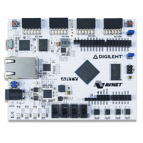
The Arty A7, formerly known as the Arty, is a ready-to-use development platform designed around the Artix-7™ Field Programmable Gate Array (FPGA) from Xilinx. It was designed specifically for use as a MicroBlaze Soft Processing System. When used in this context, the Arty A7 becomes the most flexible processing platform you could hope to add to your collection, capable of adapting to whatever your project requires. Unlike other Single Board Computers, the Arty A7 isn't bound to a single set of processing peripherals: One moment it's a communication powerhouse chock-full of UARTs, SPIs, IICs, and an Ethernet MAC, and the next it's a meticulous timekeeper with a dozen 32-bit timers.
Features
Xilinx Artix-7 FPGA
- 5,200 slices containing four 6-input LUTs and 8 flip-flops (15,850 slices)1)
- 1,800 Kbits of fast block RAM (4,860 Kbits)2)
- 5 clock management tiles (CMTs), each with a phase-locked loop and mixed-mode clock manager (6 CMTs)3)
- 90 DSP slices (240 DSP slices)4)
- Internal clock speeds exceeding 450MHz
- On-chip analog-to-digital converter (XADC)
- Programmable over JTAG and Quad-SPI Flash
System Features
- 256MB DDR3L with a 16-bit bus @ 333MHz
- 16MB Quad-SPI Flash
- USB-JTAG Programming circuitry
- Powered from USB or any 7V-15V source
System Connectivity
- 10/100 Mbps Ethernet
- USB-UART Bridge
Interaction and Sensory Devices
- 4 Switches
- 4 Buttons
- 1 Reset Button
- 4 LEDs
- 4 RGB LEDs
- Expansion Connectors
- 4 Pmod connectors
- Arduino/ChipKit Shield connector
Referneces
no_std
The application of #![no_std] at the crate level in Rust denotes a deliberate choice to link with the core crate rather than the std crate. This choice is significant in scenarios where the program aims for minimal dependencies and operates in environments without a full-fledged standard library. In this context, the libcore crate serves as a versatile foundation, offering a platform-agnostic subset of the standard library.
Libcore focuses on essential language constructs like floats, strings, and slices, providing crucial APIs for these primitives. Additionally, it exposes interfaces for low-level processor features, including atomic operations and SIMD instructions. However, it deliberately omits APIs related to platform-specific integrations, ensuring its adaptability to diverse environments.
It's worth noting that due to these characteristics, code marked as no_std and utilizing libcore finds applications beyond standard Rust environments. Yet, it is essential to recognize that such code is not suitable for tasks requiring direct interaction with specific platform features, making it unsuitable for bootstrapping activities such as building bootloaders, firmware, or kernels. This intentional abstraction provides a flexible foundation for projects that prioritize efficiency, minimalism, and portability.
Overview
| feature | no_std | std |
|---|---|---|
| heap (dynamic memory) | * | ✓ |
| collections (Vec, BTreeMap, etc) | ** | ✓ |
| stack overflow protection | ✘ | ✓ |
| runs init code before main | ✘ | ✓ |
| libstd available | ✘ | ✓ |
| libcore available | ✓ | ✓ |
| writing firmware, kernel, or bootloader code | ✓ | ✘ |
* Only if you use the alloc crate and use a suitable allocator like [alloc-cortex-m].
** Only if you use the collections crate and configure a global default allocator.
** HashMap and HashSet are not available due to a lack of a secure random number generator.
Bare Metal Environments
In the realm of bare metal programming, your program begins its execution without any pre-loaded code. Unlike environments supported by an operating system, a bare metal setup lacks the infrastructure to load the standard library. Here, the program, along with the crates it utilizes, solely interacts with the hardware—running in a "bare metal" state.
To instruct Rust not to load the standard library, the no_std attribute is employed. In this context, the platform-agnostic elements of the standard library are accessible through libcore. Notably, libcore deliberately excludes components that may not be universally suitable in an embedded environment. A prime example is the omission of a memory allocator for dynamic memory allocation.
In scenarios where additional functionalities, such as a memory allocator, are needed, numerous crates are available to fulfill these requirements. These crates extend the capabilities of bare metal programming by providing specific features while maintaining compatibility with the constraints of embedded systems.
Rust, with its emphasis on memory safety and low-level control, emerges as a valuable tool for bare metal programming. Its no_std feature, coupled with libcore, enables developers to harness the power of Rust in environments where direct hardware interaction is paramount, allowing for efficient, secure, and tailored solutions in the realm of embedded systems.
Why Rust in Shakti ?
Using Rust in the SHAKTI processor brings several advantages, aligning with Rust's strengths in system programming and embedded development. Here are key reasons for considering Rust in the context of the SHAKTI processor:
Memory Safety : Rust's ownership system and borrowing rules ensure memory safety without sacrificing performance. This is crucial in embedded systems where memory management is often critical for stability and security. Rust helps prevent common programming errors like null pointer dereferences and buffer overflows, leading to more robust and reliable code.
Zero-Cost Abstractions : Rust allows developers to write high-level, expressive code without incurring a runtime overhead. This is essential for embedded systems where resource constraints are common. The zero-cost abstractions provided by Rust enable efficient code execution without sacrificing readability or expressiveness.
Concurrency and Parallelism : Rust provides powerful abstractions for concurrent and parallel programming, making it well-suited for modern processors with multiple cores. This can enhance the performance of applications running on the SHAKTI processor, especially in scenarios where parallel processing is beneficial.
Static Typing : Rust's static typing system helps catch many common errors at compile time, reducing the likelihood of runtime failures. This is advantageous in embedded systems where debugging and maintenance can be challenging.
Community and Ecosystem : Rust has a vibrant and growing community with a focus on systems programming and embedded development. The availability of libraries, tools, and documentation makes it easier for developers working on the SHAKTI processor to find support and resources.
Cross-Platform Development : Rust supports cross-compilation, enabling developers to write code on one platform and deploy it on the SHAKTI processor or other architectures. This flexibility is beneficial for cross-platform development and porting code to different embedded systems.
Open Source and Transparency : Rust is an open-source language with a transparent development process. This aligns well with the principles of the SHAKTI project, which emphasizes openness and collaboration. The open nature of Rust fosters community involvement and innovation.
In summary, Rust's focus on safety, performance, and expressiveness, along with its strong community support, makes it a compelling choice for programming the SHAKTI processor, particularly in embedded and system-level development.
why not c ?
C is a powerful and established language in embedded systems, but Rust provides a modern and safer alternative tailored for system-level programming challenges. The decision between Rust and C hinges on project requirements, developer preferences, and the goals of the embedded system. Rust's features, such as enhanced memory safety and zero-cost abstractions, make it particularly appealing for modern processors like SHAKTI, striking a balance between performance and safety.
GDB (GNU Debugger)
GDB is a powerful debugger commonly used in embedded development. It allows developers to inspect and debug programs running on embedded systems. GDB supports various architectures, including ARM, making it suitable for debugging ARM Cortex-M microcontrollers.
Installation Steps for GDB on Linux:
open terminal
sudo apt-get install gdbgdb --version
OpenOCD (Open On-Chip Debugger)
OpenOCD acts as a bridge between GDB and the debugging hardware, such as ST-Link, on your embedded system. It facilitates communication by translating GDB's TCP/IP-based remote debug protocol to the specific protocol used by the debugging hardware.
Installation Steps for GDB and OpenOCD on Linux:
sudo apt-get install openocdopenocd --version
Rustup and Nightly
Install Rustup:
curl --proto '=https' --tlsv1.2 -sSf https://sh.rustup.rs | shsource $HOME/.cargo/env
Install Nightly:
After installing Rustup, you can install the nightly toolchain:
rustup toolchain install nightly
rustup default nightly
Add riscv target supported for Shakti
rustup target add thumbv7em-none-eabihfrustup show
Note : rustup show will show all the installed tool chains and targets, which helps to verify.
Installing & seting up FPGA
Installing Vivado
-
If you dont have a Xilinx account, create a free account, using url below:
-
Download the AMD Unified Installer for FPGAs & Adaptive SoCs 2023.2: Linux Self Extracting Web Installer from below link:
-
Make the Vivado installer executable and run it using:
chmod +x Xilinx_*.binsudo ./Xilinx_*.bin
-
Once the installer loads2
click "Next"
- Now enter your Xilinx username and password. Then Click "Next".
- Agree to all three statements and Click "Next". Incase, you disagree you can’t proceed further.
- Select "Vivado HL WebPACK or Vivado Lab " and click "Next".
- Click "Reset to Defaults" and then press "Next". 3
- By default, the "installation directory" is "/tools/Xilinx". This is the default installation directory. Click "Next".
- Click "Install" and wait for the installer to finish.
- Install the Xilinx cable drivers:
cd /tools/Xilinx/Vivado/2018.3/data/xicom/cable_drivers/lin64/install_script/install_driverssudo ./install_drivers
- Do some permissions cleanup:
cdcd .Xilinx/Vivadosudo chown -R $USER *sudo chmod -R 777 *sudo chgrp -R $USER *
- Add Vivado path to the environmental variable PATH in .bashrc :
export PATH=$PATH:/tools/Xilinx/Vivado/2018.3/binexport PATH=$PATH:/tools/Xilinx/SDK/2018.3/bin
- Test Vivado
vivado -version
Programming Arty-7 FPGA
Refer shakti user manual to program the board.
SHAKTI, a groundbreaking RISC-V-based processor, introduces the E and C-classes—representing the initial set of indigenous designs tailored for the Internet of Things (IoT), Embedded Systems, and Desktop markets. Emphasizing an open and collaborative approach, the processor design is devoid of royalties and released under the BSD3 license. SHAKTI's E and C-classes provide a foundation for innovative processor architectures with diverse applications.
E-Class
The 32-bit E-Class microprocessor is designed for low-power compute environments, automotive, and IoT applications. Operating on an in-order 3-stage pipeline below 200MHz, it supports all RISC-V ISA extensions. Noteworthy for running Real-Time Operating Systems (RTOS) like Zephyr OS and FreeRTOS, the E-Class competes with ARM's M-class cores. Key applications include smart cards, motor controls, and home automation.
PINAKA (E32-A35): PINAKA, built around the E-Class, is a 32-bit microcontroller with 4KB ROM and 128KB BRAM. Featuring 32 GPIO pins (8 for onboard LEDs and switches), it includes a Platform Level Interrupt Controller (PLIC), Timer (CLINT), 2 SPI, 3 UART, 2 I2C, 6 PWM, Xilinx ADC, Soft Float library, Physical Memory Protection (PMP), an onboard FTDI-based debugger, and Pin Mux support with Arduino-compatible assignments.
PARASHU (E32-A100): Sharing the E-Class configuration, PARASHU is a 32-bit microcontroller with 4KB ROM and 256MB DDR. Suited for various applications, it provides additional memory capacity.
C-Class
The 64-bit C-Class, a 6-stage microcontroller, supports the entire RISC-V ISA. Customizable for 200-800MHz mid-range compute systems, it competes with ARM's Cortex A35/A55. Compatible with Linux, SEL4, and FreeRTOS, the C-Class caters to both low-power and high-performance variants.
VAJRA (C64-A100): VAJRA, built around the C-Class, is a single-chip 64-bit microcontroller with 4KB ROM and 256MB DDR3 RAM. Targeted at mid-range applications like industrial controllers and the desktop market, VAJRA shares a configuration with PARASHU.
Peripherals
| Peripherals | info |
|---|---|
| GPIO Pins | 32 |
| Upper | 8 pins Onboard LEDs and switches |
| PLIC | 1 |
| Counter | 1 |
| SPI | 2 |
| UART | 3 |
| I2C | 2 |
| PWM | 6 |
| ADC | Xilinx |
| CLINT | 1 |
| Float | Soft library |
| PMP | Enabled |
| Debugger | Onboard FTDI based |
| Pin Mux | Yes |
| Ethernet lite | PARASHU, VAJRA |
GPIO
The GPIO functionality in the SHAKTI processor is a versatile feature, enabling the generation of custom waveforms, activation of signals, and handling interrupts. Here are additional details about the GPIO operation:
GPIO Registers
-
GPIO DIRECTION Register: The GPIO DIRECTION register configures the GPIO pin as either an input or output. This register plays a crucial role in determining the operational mode of the GPIO pins.
-
GPIO DATA Register: The GPIO DATA register holds the input data from GPIO or the output data to GPIO. It is accessible in 1-byte, 2-byte, and 4-byte sizes, providing flexibility in data manipulation.
-
Interrupt Handling (GPIO Pins 0 - 7): GPIO pins 0 - 7 can accept external events as interrupts. To use a GPIO pin as an interrupt source, the respective GPIO pin(s) must be configured as inputs. This feature enhances the processor's ability to respond to external stimuli.
GPIO Registers:
-
GPIO_DIRECTION_CNTRL_REG (Offset 'h00): This 32-bit register controls the direction of GPIO pins, allowing configuration as either input or output. It supports both read and write operations.
-
GPIO_DATA_REG (`h08): This register, accessible in 32, 16, or 8 bits, serves as the GPIO Data Register. It supports read and write operations, facilitating data handling for GPIO pins.
-
Sequence of Execution:
- To effectively utilize the GPIO functionality, follow this sequence:
- Write into the GPIO Direction register (GPIO_DIRECTION_CNTRL_REG) to configure the GPIO pin as an input or output.
- Write appropriate values to the GPIO Data register (GPIO_DATA_REG) based on the desired input or output data.
These steps ensure proper configuration and operation of the GPIO pins, making them valuable for a wide range of applications in signal processing and interrupt-driven scenarios.
- To effectively utilize the GPIO functionality, follow this sequence:
Rust GPIO Register implmentation
use crate::common::MMIODerefWrapper;
use riscv::{
    asm::{delay, nop},
    register,
};
use tock_registers::{
    interfaces::{Readable, Writeable},
    register_bitfields, register_structs,
    registers::{ReadOnly, ReadWrite, WriteOnly},
};

//--------------------------------------------------------------------------------------------------
// Private Definitions
//--------------------------------------------------------------------------------------------------

pub const GPIO_OFFSET: usize = 0x0004_0100;

register_structs! {
    #[allow(non_snake_case)]
    pub RegistersBlock{
        (0x00 => DIRECTION_CR_REG: ReadWrite<u32>),
        (0x04 => _reserved0),
        (0x08 => DATA_REG: ReadWrite<u32>),
        (0x0C => @END),
    }
}

register_bitfields! {
    u32,

    DIRECTION_CR_REG [
        CR OFFSET(0) NUMBITS(32) []
    ],
    SCL[
        DATA_REG OFFSET(0) NUMBITS(32) []
    ],

}

type Registers = MMIODerefWrapper<RegistersBlock>;

pub struct GPIOInner {
    registers: Registers,
}
- Memory-Mapped I/O (MMIO):
use crate::common::MMIODerefWrapper: Imports a wrapper for MMIO, which is a technique for interfacing with hardware registers by mapping them to specific memory addresses.
- RISC-V Assembly and Registers:
use riscv::{asm::{delay, nop}, register}: Imports RISC-V assembly instructions (delay, nop) and register-related functionality. RISC-V is an instruction set architecture commonly used in embedded systems.
- Tock Registers:
use tock_registers::{interfaces::{Readable, Writeable}, register_bitfields, register_structs, registers::{ReadOnly, ReadWrite, WriteOnly}};: Imports Tock Registers, a library for working with hardware registers in embedded systems. It provides traits for reading and writing registers, as well as utilities for defining register bitfields.
- GPIO Offset:
pub const GPIO_OFFSET: usize = 0x0004_0100;: Defines the offset for GPIO registers in memory.
- Register Block Definition:
register_structs! { ... }: Defines a block of memory-mapped registers for GPIO. This includes the Direction Control Register (DIRECTION_CR_REG) and Data Register (DATA_REG), specifying their offsets and types.
- Register Bitfields:
register_bitfields! { ... }: Defines specific bitfields within the registers, such as the CR field in the Direction Control Register and the DATA_REG field in the Data Register.
- Registers Wrapper:
type Registers = MMIODerefWrapper
- GPIOInner Structure:
pub struct GPIOInner { registers: Registers, }: Defines a structure encapsulating the GPIO registers. This structure is likely used to abstract GPIO operations and provide a more organized interface.
UART
The UART module in the Shakti SoC (System on Chip) provides asynchronous serial communication with RS-232 (RS-422/485) interface. It operates in a non-return-to-zero (NRZ) mode, supporting data transfer rates that can be configured through the UARTBAUD register. Here's a concise overview of key UART registers and their functionalities:
UART Registers
- BAUD Register (Address: 0x00) Configures the Baud rate based on the set Baud value. Baud Rate calculation: Baud_value = (Clock Frequency) / (16 * Baudrate)
- Status Register (Address: 0x0C) Provides status information about transmit and receive operations. Break, frame, overrun, and parity error flags. Flags indicating receiver and transmitter buffer status.
- Control Register (Address: 0x14) Configures UART operation, character size, parity, and stop bits. Character size (data length), parity, and stop bits settings.
- TX_REG Register (Address: 0x04) Write-only register for transmitting data. Data to be transmitted is written into this register.
- RCV_REG Register (Address: 0x08) Read-only register for receiving data. The received value can be read from this register.
- IEN Register (Address: 0x18) Enables interrupts based on the set bit values in the Interrupt Enable Register. Interrupts for various conditions like threshold, break error, frame error, overrun, parity error, and buffer status.
- DELAY Register (Address: 0x10) Controls delayed transmit by specifying the required delay count.
- IQCYCLES Register (Address: 0x1C) Holds the number of input qualification cycles for the receiver pin.
- RX_THRESHOLD Register (Address: 0x20) Holds the receiver FIFO threshold value. Generates corresponding status bits and interrupts when the FIFO level crosses the threshold. These registers collectively define the configuration, status, and control aspects of the UART module in the Shakti SoC, facilitating efficient and configurable serial communication.
Rust UART Register implmentation
use crate::common::MMIODerefWrapper;
use riscv::{
    asm::{delay, nop},
    register,
};
use tock_registers::{
    interfaces::{Readable, Writeable},
    register_bitfields, register_structs,
    registers::{ReadOnly, ReadWrite, WriteOnly},
};

//--------------------------------------------------------------------------------------------------
// Private Definitions
//--------------------------------------------------------------------------------------------------

pub const UART_OFFSET: usize = 0x0001_1300;
pub const STS_TX_FULL_FLAG: u8 = 0x02;
pub const STS_RX_NOT_EMPTY_FLAG: u8 = 0x08;

pub const BREAK_ERROR: u8 = 1 << 7;
pub const FRAME_ERROR: u8 = 1 << 6;
pub const OVERRUN: u8 = 1 << 5;
pub const PARITY_ERROR: u8 = 1 << 4;
pub const STS_RX_FULL: u8 = 1 << 3;
pub const STS_RX_NOT_EMPTY: u8 = 1 << 2;
pub const STS_TX_FULL: u8 = 1 << 1;
pub const STS_TX_EMPTY: u8 = 1 << 0;

register_structs! {
    #[allow(non_snake_case)]
    pub RegistersBlock{
        (0x00 => UBR: ReadWrite<u16>),
        (0x02 => _reserved0),
        (0x04 => TX_REG: WriteOnly<u32>),
        (0x08 => RCV_REG: ReadOnly<u32, RCV_REG::Register>),
        (0x0C => USR : ReadOnly<u8, USR::Register>),
        (0x0D => _reserved1),
        //(0x0E => _reserved2),
        (0x10 => DELAY: ReadWrite<u32, DELAY::Register>),
        // (0x12 => _reserved3),
        (0x14 => UCR: ReadWrite<u32, UCR::Register>),
        // (0x16 => _reserved4),
        (0x18 => IEN: ReadWrite<u32, IEN::Register>),
        // (0x1A => _reserved5),
        (0x1C => IQCYCLES: ReadWrite<u32, IQCYCLES::Register>),
        // (0x1D => _reserved6),
        // (0x1E => _reserved7),
        // (0x1F => _reserved11),
        (0x20 => RX_THRESHOLD: WriteOnly<u32, RX_THRESHOLD::Register>),
        // (0x21 => _reserved8),
        // (0x22 => _reserved9),
        // (0x23 => _reserved10),
        (0x24 => @END),
    }
}

register_bitfields! {
    u32,

    UBR [
        BAUD OFFSET(0) NUMBITS(16) []
    ],

    /// UART Status register
    USR [
        /// Transmit FIFO empty. The meaning of this bit depends on the state of the FEN bit in the
        /// Line Control Register, LCR_H.
        ///
        /// - If the FIFO is disabled, this bit is set when the transmit holding register is empty.
        /// - If the FIFO is enabled, the TXFE bit is set when the transmit FIFO is empty.
        /// - This bit does not indicate if there is data in the transmit shift register.
        BREAK_ERROR OFFSET(7) NUMBITS(1) [],
        ///Break Error (Sets when the data and stop are both zero
        FRAME_ERROR OFFSET(6) NUMBITS(1) [],
        ///Frame Error (Sets when the stopis zero)
        OVERRUN OFFSET(5) NUMBITS(1) [],
        ///Overrun Error (A data overrun error occurred in the receive
        ///shift register. This happens when additional data arrives
        ///while the FIFO is full. )
        PARITY_ERROR OFFSET(4) NUMBITS(1) [],
        ///Parity Error (Sets when The receive character does not
        ///have correct parity information and is suspect.

        STS_RX_FULL OFFSET(3) NUMBITS(1) [],
        ///Receiver Full (Sets when the Receive Buffer is Full)

        STS_RX_NOT_FULL OFFSET(2) NUMBITS(1) [],
        /// Receiver Not Empty (Sets when there is some data in the
        ///Receive Buffer).
        STS_TX_FULL OFFSET(1) NUMBITS(1) [
            EMPTY = 0,
            FULL = 1,
        ],
        ///Transmitter Full (Sets when the transmit Buffer is full)
        STS_TX_EMPTY OFFSET(0) NUMBITS(1) [
            EMPTY = 1,
            FULL = 0,
        ]
        //Transmitter Empty(Sets when the Transmit Buffer is empty).
    ],

    UCR [
        UART_TX_RX_LEN OFFSET(5) NUMBITS(6) [],
        //Character size of data. Maximum length is 32 bits.
        PARITY OFFSET(3) NUMBITS(2) [
            None = 0b00,
            Odd = 0b01,
            Even = 0b10,
            Unused = 0b11

        ],
         //Insert Parity bits
         //00 - None
         //01 - Odd
        //10- Even
        // 11 - Unused or Undefined
        STOP_BITS OFFSET(1) NUMBITS(2) [

            StopBits1 = 0b00,
            StopBits1_5 = 0b01,
            StopBits2 = 0b10


        ],
        //Stop bits
       //00 - 1 Stop bits
        //01 - 1.5 Stop bits
        //10 - 2 Stop bits
    ],

    TX_REG [

        TX_DATA OFFSET(0) NUMBITS(32) []
    ],


    RCV_REG [

        RX_DATA OFFSET(0) NUMBITS(32) []
    ],

    IEN [

        ENABLE_TX_EMPTY OFFSET(0) NUMBITS(1) [],
        ENABLE_TX_FULL OFFSET(1) NUMBITS(1) [],
        ENABLE_RX_NOT_EMPTY OFFSET(2) NUMBITS(1) [],
        ENABLE_RX_FULL OFFSET(3) NUMBITS(1) [],
        ENABLE_PARITY_ERROR OFFSET(4) NUMBITS(1) [],
        ENABLE_OVERRUN OFFSET(5) NUMBITS(1) [],
        ENABLE_FRAME_ERROR OFFSET(6) NUMBITS(1) [],
        ENABLE_BREAK_ERROR OFFSET(7) NUMBITS(1) [],
        ENABLE_RX_THRESHOLD OFFSET(8) NUMBITS(1) []
    ],
///Delayed Transmit control is done by providing the required delay in UART DELAY register.
      DELAY [
        COUNT OFFSET(0) NUMBITS(8) []
      ],
///UART IQCYCLES Register holds the number of input qualification cycles for the receiver pin. .
      IQCYCLES[
        COUNT OFFSET(0) NUMBITS(8) []
      ],
    RX_THRESHOLD [
        /// UART RX_THRESHOLD register holds the receiver FIFO threshold value, when the RX FIFO
        ///level increases beyond the threshold, corresponding status bit will be set and when interrupt is
       ///enabled, interrupt will be raised
        FIFO_RX OFFSET(0) NUMBITS(8) []
    ]

}
/// Abstraction for the associated MMIO registers.
type Registers = MMIODerefWrapper<RegistersBlock>;

pub struct UartInner {
    registers: Registers,
}
- Dependencies:
The code relies on the MMIODerefWrapper from the common module. It uses various modules and traits from the riscv and tock_registers crates.
- Register Definitions:
The RegistersBlock struct defines memory-mapped I/O (MMIO) registers for the UART module. Register addresses and their offsets are specified, along with their bitfields.
- Constants:
UART_OFFSET: Specifies the offset for the UART module in memory. Flags and error constants such as STS_TX_FULL_FLAG, STS_RX_NOT_EMPTY_FLAG, BREAK_ERROR, etc., are defined.
- Register Bitfields:
The register_bitfields! macro is used to define bitfields for various registers. It provides convenient access to specific bits within the registers.
- Register Types:
Read, Write, and ReadWrite traits are implemented for certain register types, indicating their accessibility.
- Structs:
RegistersBlock: Represents the MMIO registers for the UART module. UartInner: Encapsulates the inner workings of the UART, including access to MMIO registers.
- Struct Initialization:
Registers: A wrapper around RegistersBlock, providing safe access to the MMIO registers. UartInner: Contains a Registers instance.
This code essentially establishes a clear abstraction for working with the UART module in the Shakti RISC-V processor, allowing developers to interact with the UART hardware through safe and well-defined Rust abstractions.
SPI
The SPI (Serial Peripheral Interface) is a synchronous serial I/O (Input/Output) port commonly used for communication between microcontrollers and peripheral devices. Here's a breakdown of the SPI registers for a Shakti RISC-V processor:
SPI Registers
- SPI_CR1 (Offset: 'h00) : 32 bits, Read and Write - SPI Control Register 1.
- SPI_CR2 (Offset: 'h04) : 32 bits, Read and Write - SPI Control Register 2.
- SPI_SR (Offset: 'h08) : 32 bits, Read Only - SPI Status Register.
- SPI_DR1 (Offset: 'h0C) : 32 bits, Read and Write - SPI Data Register 1.
- SPI_DR2 (Offset: 'h10) : 32 bits, Read and Write - SPI Data Register 2.
- SPI_DR3 (Offset: 'h14) : 32 bits, Read and Write - SPI Data Register 3.
- SPI_DR4 (Offset: 'h18) : 32 bits, Read and Write - SPI Data Register 4.
- SPI_DR5 (Offset: 'h1C) : 32 bits, Read and Write - SPI Data Register 5.
- SPI_CRCPR (Offset: 'h20) : 32 bits, Reserved - SPI CRC Polynomial Register.
- SPI_RXCRCR (Offset: 'h24): 32 bits, Reserved - SPI RX CRC Register.
- SPI_TXCRCR (Offset: 'h28): 32 bits, Reserved - SPI TX CRC Register.
These registers control various aspects of the SPI module, including data transfer, CRC (Cyclic Redundancy Check), and status information. Developers can interact with these registers to configure and manage SPI communication in their applications.
Rust SPI Register implmentation
use riscv::asm::delay;
use tock_registers::{
    fields::FieldValue,
    interfaces::{ReadWriteable, Readable, Writeable},
    register_bitfields, register_structs,
    registers::{ReadOnly, ReadWrite, WriteOnly},
};

use crate::common::MMIODerefWrapper;

use self::SPI_CR1::SPI_TOTAL_BITS_TX;

pub const SPI_OFFSET: usize = 0x0002_0000;

register_bitfields! {
    u32,

    SPI_CR1 [

        /// Expected Total Number of bits to be received.
        SPI_TOTAL_BITS_RX OFFSET(24) NUMBITS(8) [

        ],

        /// Total Number of bits to be transmitted.
        SPI_TOTAL_BITS_TX OFFSET(16) NUMBITS(8) [

        ],

        /// Bidirectional data mode enable. This bit enables
        /// half-duplex communication using a common single
        /// bidirectional data line.
        /// 0: 2-line unidirectional data mode selected
        /// 1: 1-line unidirectional data mode selected
        SPI_BIDIMODE OFFSET(15) NUMBITS(1) [
            OUTPUT_ENABLE = 1,
            PUTPUT_DISABLE = 0,
        ],

        /// Output enable in bidirectional mode This bit combined with
        /// the BIDI-MODE bit selects the direction of transfer in bi-direction mode.
        /// 0: receive-only mode (Output Disabled)
        /// 1: transmit-only mode (Output Enabled)
        SPI_BIDIODE OFFSET(14) NUMBITS(1) [
            OUTPUT_ENABLE = 1,
            PUTPUT_DISABLE = 0,
        ],


        /// Hardware CRC calculation Enable.
        /// 0: CRC calculation disable
        /// 1: CRC calculation enable
        SPI_CRCEN OFFSET(13) NUMBITS(1) [
            HWCRC_ENABLE = 1,
            HWCRC_DISABLE = 0,
        ],

        /// Transmit CRC Next.
        /// 0: Next Transmit value is from Tx buffer
        /// 1: Next Transmit value is from Rx buffer
        SPI_CCRCNEXT OFFSET(12) NUMBITS(1) [
            CRCNEXT_RX = 1,
            CRCNEXT_TX = 0,
        ],

        /// CRC Length bit is set and cleared by software to select CRC Length
        SPI_CRCL OFFSET(11) NUMBITS(1) [

        ],

        /// Receive only mode enabled. This bit enables simplex
        /// communication using a single unidirectional line to
        /// receive data exclusively. Keep BIDIMODE bit clear when
        /// receiving the only mode is active.
        SPI_RXONLY OFFSET(10) NUMBITS(1) [

        ],

        /// Software Slave Management. When the SSM bit is set,
        /// the NSS pin input is replaced with the value from the SSI
        /// bit.
        /// 0: Software slave management disabled
        /// 1: Software slave management enabled
        SPI_SSM OFFSET(9) NUMBITS(1) [
            SSM_ENABLED  = 1,
            SSM_DISABLED = 0,
        ],

        /// Internal Slave Select.This bit has an effect only when the
        /// SSM bit is set. The value of this bit is forced onto the
        /// NSS pin and the I/O value of the NSS pin is ignored
        SPI_SSI OFFSET(8) NUMBITS(1) [

        ],

        /// Frame Format
        /// 0: data is transmitted/received with the MSB first
        /// 1: data is transmitted/received with the LSB first
        /// Note: This bit should not be changed when communication is ongoing
        SPI_LSBFIRST OFFSET(7) NUMBITS(1) [
            LSB_FIRST = 1,
            MSB_FIRST = 0,
        ],

        /// SPI Enable
        /// 0: SPI is disabled
        /// 1: SPI is enabled
        SPI_SPE OFFSET(6) NUMBITS(1) [
            ENABLED  = 1,
            DISABLED = 0,
        ],

        /// Baud Rate Control
        /// 000: fCLK/2
        /// 001: fCLK/4
        /// 010: fCLK/8
        /// 011: fCLK/16
        /// 100: fCLK/32
        /// 101: fCLK/64
        /// 110: fCLK/128
        /// 111: fCLK/256
        /// Note:This bit should not be changed when communication is ongoing
        SPI_BR OFFSET(3) NUMBITS(3) [

        ],

        /// Master Selection
        /// 0: Slave Configuration
        /// 1: Master Configuration
        /// Note This bit should not be changed when communication is ongoing
        SPI_MSTR OFFSET(2) NUMBITS(1) [
            SLAVE_CONFIG   = 1,
            MASTER_CONFIG  = 0,
        ],

        ///Clock Polarity
        ///0: CLK is 0 when idle
        ///1: CLK is 1 when idle
        SPI_CPOL OFFSET(1) NUMBITS(1) [
            ONE_IDLE   = 1,
            ZERO_IDLE  = 0,
        ],

        ///Clock Phase
        ///0: The first clock transition is the first data capture edge
        ///1: The second clock transition is the first data capture edge
        SPI_CPHA OFFSET(0) NUMBITS(1) [
            SECOND_CLK = 1,
            FIRST_CLK  = 0,
        ]
    ],

    SPI_CR2 [
        ///SPI_TOTAL_BITS_RX OFFSET(24) NUMBITS(7) [],
        SPI_RX_IMM_START OFFSET(16) NUMBITS(1) [],
        SPI_RX_START OFFSET(15) NUMBITS(1) [],
        SPI_LDMA_TX_START OFFSET(14) NUMBITS(1) [],
        SPI_LDMA_RX OFFSET(13) NUMBITS(1) [],

        /// FIFO reception threshold is used to set the threshold of
        /// the RXFIFO that triggers an RXNE event.
        /// 0: RXNE event is generated if the FIFO level is greater
        /// than or equal to 1/2 (16-bit)
        /// 1: RXNE event is generated if the FIFO level is greater
        /// than or equal to 1/4 (8-bit)
        SPI_FRXTH OFFSET(12) NUMBITS(1) [],

        /// Reserved bits
        /// SPI_DS OFFSET(8) NUMBITS(4) [],

        /// Interrupt enable for TXE event.
        /// 0: TXE interrupt masked
        /// 1: TXE interrupt is not interrupt masked
        SPI_TXEIE OFFSET(7) NUMBITS(1) [],

        /// Interrupt enable for RXNE event
        /// 0: RXNE interrupt masked
        /// 1: RXNE interrupt is not interrupt masked
        SPI_RXNEIE OFFSET(6) NUMBITS(1) [
            RXNE_UNMASKED = 1,
            RXNE_MASKED = 0,
        ],

        /// when an error condition occurs.
        /// 0: Error interrupt masked
        /// 1: Error interrupt not masked.
        //Frame Error (Sets when the stopis zero)
        SPI_ERRIE OFFSET(5) NUMBITS(1) [
            MASKED_INT   = 1,
            UNMASKED_INT = 0,
        ],

        /// Reserved bits
        /// SPI_FRF OFFSET(4) NUMBITS(1) [],
        /// SPI_NSSP OFFSET(3) NUMBITS(1) [],

        /// SS output enable
        /// 0: SS output is disabled in master mode and the SPI interface
        /// can work in a multi-master configuration
        /// 1: SS output is enabled in master mode and when the SPI
        /// interface is enabled. The SPI interface cannot work in a
        /// multi-master environment.
        SPI_SSOE OFFSET(2) NUMBITS(1) [
            SSOE_ENABLED  = 1,
            SSOE_DISABLED = 0,
        ],

        // Reserved bits
        // SPI_TXDMAEN OFFSET(1) NUMBITS(1) [],
        // SPI_RXDMAEN OFFSET(0) NUMBITS(1) [],

    ],

    SPI_SR[

        SPI_FTLVL OFFSET(11) NUMBITS(2) [],
        SPI_FRLVL OFFSET(9) NUMBITS(2) [],

        SPI_FRE OFFSET(8) NUMBITS(1) [],
        SPI_BSY OFFSET(7) NUMBITS(1) [],
        SPI_OVR OFFSET(6) NUMBITS(1) [],

        SPI_MODF OFFSET(5) NUMBITS(1) [],

        SPI_CRCERR OFFSET(4) NUMBITS(1) [],

        SPI_TXE OFFSET(1) NUMBITS(1) [],

        SPI_RXNE OFFSET(0) NUMBITS(1) []

    ],

    SPI_DR1 [
        DR1 OFFSET(0) NUMBITS(32) []
    ],

    SPI_DR2 [
        DR2 OFFSET(0) NUMBITS(32) []
    ],

    SPI_DR3 [
        DR3 OFFSET(0) NUMBITS(32) []
    ],

    SPI_DR4 [
        DR4 OFFSET(0) NUMBITS(32) []
    ],

    SPI_DR5 [
        DR5 OFFSET(0) NUMBITS(32) []
    ],


}

register_structs! {
    #[allow(non_snake_case)]
    pub RegisterBlock{
        (0x00 => SPI_CR1: ReadWrite<u32, SPI_CR1::Register>),
        (0x04 => SPI_CR2: ReadWrite<u32, SPI_CR2::Register>),
        (0x08 => SPI_SR:  ReadOnly <u32, SPI_SR ::Register>),
        (0x0C => SPI_DR1: ReadWrite <u32, SPI_DR1::Register>),
        (0x10 => SPI_DR2: ReadWrite <u32, SPI_DR2::Register>),
        (0x14 => SPI_DR3: ReadWrite <u32, SPI_DR3::Register>),
        (0x18 => SPI_DR4: ReadWrite <u32, SPI_DR4::Register>),
        (0x1C => SPI_DR5: ReadWrite <u32, SPI_DR5::Register>),
        (0x20 => _reserved),
        (0x2C => @END),
    }
}

/// Abstraction for the associated MMIO registers.
type Registers = MMIODerefWrapper<RegisterBlock>;

pub struct SPIInner {
    registers: Registers,
}
The code includes necessary dependencies from tock_registers and defines a constant SPI_OFFSET representing the memory-mapped offset for the SPI module.
Bitfields Definition The code defines bitfields for various SPI registers (SPI_CR1, SPI_CR2, SPI_SR, SPI_DR1, SPI_DR2, SPI_DR3, SPI_DR4, SPI_DR5). Each register has different bitfields representing configuration options and status flags.
Register Structures The code uses the register_structs! macro to define the memory-mapped register block for the SPI module. It includes registers like SPI_CR1, SPI_CR2, SPI_SR, SPI_DR1, SPI_DR2, SPI_DR3, SPI_DR4, and SPI_DR5. Each register is associated with its offset in memory, and their types are specified based on read or write access and the bitfields defined earlier.
SPIInner Struct
The SPIInner struct is defined to encapsulate the SPI module's registers. It contains a field registers of type MMIODerefWrapper
Overall, the code sets up a structured representation of the SPI module's registers with bitfields and provides an abstraction (SPIInner) for interacting with these registers. It's a common pattern in embedded systems programming to use such abstractions to manage hardware peripherals.
I2C
Shakti processors, which are based on the RISC-V architecture, the I2C (Inter-Integrated Circuit) interface is commonly used to connect low-speed devices within embedded systems. The I2C module in Shakti processors typically includes several registers that control and manage the communication on the I2C bus. Here's a general overview of the I2C module for Shakti:
I2C Registers:
-
Prescale Register (Prescale - Offset 0x00): Size: 8 bits Accessible: Read/Write Description: Configures the I2C prescaler, which divides the system clock to determine the I2C clock frequency.
-
Control Register (Control - Offset 0x08): Size: 8 bits Accessible: Read/Write Description: Configures and controls the I2C data transfer. Key bits include: I2C_PIN: Pending Interrupt Not, Used as a software reset. I2C_ENI: Enables the external interrupt output. I2C_STA: Transmits Start condition + Slave address. I2C_STO: Transmits the stop condition. I2C_ACK: Acknowledgement bit.
-
Data Shift Register (Data - Offset 0x10): Size: 8 bits Accessible: Read/Write Description: Holds the data to be transmitted or received during I2C communication.
-
Status Register (Status - Offset 0x18): Size: 8 bits Accessible: Read Description: Provides the status of I2C data transfer. Key bits include: I2C_INI: High when I2C communication is in progress. I2C_STS: Status flag in slave receiver mode for externally generated STOP condition. I2C_BER: Bus error flag for misplaced START or STOP condition. I2C_AD0/I2C_LRB: Last Received Bit and Address 0 in slave mode. I2C_AAS: Addressed As Slave bit. I2C_LAB: Lost Arbitration Bit. I2C_BB: Bus Busy bit.
-
Clock Register (SCL - Offset 0x38): Size: 8 bits Accessible: Read/Write Description: Divides the I2C Prescaler clock to determine the I2C SCL (Serial Clock Line) frequency.
-
General Overview:
- I2C is used for connecting low-speed devices in embedded systems.
- It facilitates communication between a single master and multiple slave devices.
- Two-wire interface: SDA (Data) and SCL (Clock).
- Each device has a unique address.
- Synchronous communication with master controlling the clock.
- Registers control prescaling, data transfer, status, and clock frequency.
Rust I2C Register implmentation
use crate::common::MMIODerefWrapper;
use riscv::{
    asm::{delay, nop},
    register,
};
use tock_registers::{
    interfaces::{Readable, Writeable},
    register_bitfields, register_structs,
    registers::{ReadOnly, ReadWrite, WriteOnly},
};

//--------------------------------------------------------------------------------------------------
// Private Definitions
//--------------------------------------------------------------------------------------------------

pub const I2C_OFFSET: usize = 0x0004_0000;

pub const I2C_INI: u8 = 1 << 7;
pub const I2C_STS: u8 = 1 << 5;
pub const I2C_BER: u8 = 1 << 4;
pub const I2C_AD0_LRB: u8 = 1 << 3;
pub const I2C_AAS: u8 = 1 << 2;
pub const I2C_LAB: u8 = 1 << 1;
pub const I2C_BB: u8 = 1 << 0;

pub const I2C_PIN: u8 = 1 << 7;
pub const I2C_ES0: u8 = 1 << 6;
pub const I2C_ENI_LRB: u8 = 1 << 3;
pub const I2C_STA: u8 = 1 << 2;
pub const I2C_STO: u8 = 1 << 1;
pub const I2C_ACK: u8 = 1 << 0;

register_structs! {
    #[allow(non_snake_case)]
    pub RegistersBlock{
        (0x00 => PRESCALE: ReadWrite<u16>),
        (0x02 => _reserved0),
        (0x08 => CONTROL: ReadWrite<u8>),
        (0x09 => _reserved1),
        (0x10 => DATA: ReadWrite<u8>),
        (0x11 => _reserved2),
        (0x18 => STATUS : ReadWrite<u8>),
        (0x19 => _reserved3),
        (0x38 => SCL : ReadWrite<u8>),
        (0x39 => _reserved4)
,       (0x3C => @END),
    }
}

register_bitfields! {
    u32,
///I2C Prescale Register divides the System clock by (Prescale value + 1). This clock is used as
///clock input for I2C Serial Clock.
///I2C Prescaler clock = System Clock / (Prescaler Value + 1)
    PRESCALE [
        PRESCALE_VALUE OFFSET(0) NUMBITS(8) []
    ],
    ///I2C SCL Register divides the I2C Prescaler clock by (SCL value + 1). This clock is used as
///I2C SCL clock = I2C Prescaler Clock / (SCL COUNT + 1).
    SCL[
        SCL_COUNT OFFSET(0) NUMBITS(8) []
    ],
    STATUS [
///High when I2C communication in progress. Becomes low once I2C
///communication is complete.
        I2C_INI OFFSET(7) NUMBITS(1) [],
   ///     When in slave receiver mode, this flag is asserted when an
      ///  externally generated STOP condition is detected (used only in
       /// slave receiver mode).
        I2C_STS OFFSET(5) NUMBITS(1) [],
///Bus error; a misplaced START or STOP condition has been
///detected
        I2C_BER OFFSET(4) NUMBITS(1) [],
     /*    AD0(Address 0) - General Call bit used for Broadcast
        LRB - Last Received Bit through I2C Bus
        This status bit serves a dual function, and is valid only while
        PIN = 0:
        1. LRB holds the value of the last received bit over the
        I2C-bus while AAS = 0 (not addressed as slave). Normally
        this will be the value of the slave acknowledgement; thus
        checking for slave acknowledgement is done via testing of the
        LRB.
        2. AD0; when AAS = 1 (‘Addressed As Slave’ condition), the
        I2C-bus controller has been addressed as a slave. Under this
        condition, this bit becomes the ‘AD0’ bit and will be set to
        logic 1 if the slave address received was the ‘general call’
        (00H) address, or logic 0 if it was the I2C-bus controller’s own
        slave address.
        */
        I2C_AD0_LRB OFFSET(3) NUMBITS(1) [],
///Addressed As Slave’ bit. Valid only when PIN = 0. When
///acting as slave receiver, this flag is set when an incoming
///address over the I2C-bus matches the value in own address
//register
        I2C_AAS OFFSET(2) NUMBITS(1) [],
///Lost Arbitration Bit. This bit is set when, in multi-master
///operation, arbitration is lost to another master on the I2C-bus
        I2C_LAB OFFSET(1) NUMBITS(1) [],
///Bus Busy bit. This is a read-only flag indicating when the
///I2C-bus is in use. A zero indicates that the bus is busy, and
///access is not possible
        I2C_BB OFFSET(0) NUMBITS(1) []

    ],

    CONTROL [
///Pending Interrupt Not, Used as a software reset. If set to 1, all
    I2C_PIN OFFSET(7) NUMBITS(1) [],
   /// Enable Serial Output.
    ///0 - Registers can be initialized.
    ///1 - I2C Serial Transmission
    I2C_ES0 OFFSET(6) NUMBITS(1) [
        REGISTER_INITIALIZED = 0,
        I2C_SERIAL_TRANSMISSION = 1,
    ],
///Enables the external interrupt output, which is generated when
///the PIN is active (Low)
    I2C_ENI OFFSET(3) NUMBITS(1) [],
///Transmits Start condition + Slave address..
    I2C_STA OFFSET(2) NUMBITS(1) [],
///Transmits the stop condition.
    I2C_STO OFFSET(1) NUMBITS(1) [],
///Acknowledgement bit.
///1: I2C automatically sends an acknowledgement after a
///read/write transaction.
///0: I2C Master sends Negative Acknowledge to stop the I2C
///transfer
    I2C_ACK OFFSET(0) NUMBITS(1) [
        NAK = 0,
        ACK = 1,
    ]

],


}

type Registers = MMIODerefWrapper<RegistersBlock>;

pub struct I2CInner {
    registers: Registers,
}
Rust implementation for interacting with the I2C (Inter-Integrated Circuit) module on Shakti processors.
-
Constants:
- I2C_OFFSET: Specifies the offset address for the I2C module in memory.
- Various constants (I2C_INI, I2C_STS, etc.) represent bit positions in status and control registers.
-
Register Structures
- RegistersBlock : Defines the memory-mapped I2C registers.
- PRESCALE : Configures the I2C prescaler for clock frequency.
- CONTROL : Configures and controls I2C data transfer.
- DATA : Holds data to be transmitted or received.
- STATUS : Provides status information about I2C communication.
- SCL : Configures the I2C SCL (Serial Clock Line) clock. -Register Bitfields:
- register_bitfields! macro defines specific bits within registers.
- PRESCALE: PRESCALE_VALUE represents the prescaler value.
- SCL : SCL_COUNT represents the count for dividing the I2C Prescaler clock.
- STATUS : Defines various status bits such as **I2C_INI, I2C_STS, I2C_BER, **etc.
- CONTROL : Defines control bits such as **I2C_PIN, I2C_ES0, I2C_ENI, **etc.
-
MMIODerefWrapper and Structs:
- MMIODerefWrapper : Represents a memory-mapped I/O (MMIO) wrapper for safe interaction with hardware registers.
- Registers : A wrapper for the RegistersBlock, ensuring safe access to I2C registers.
-
I2CInner Struct:
- I2CInner: A struct encapsulating the I2C module, containing an instance of the Registers wrapper.
PWM
Pulse Width Modulators (PWM) are used for generating pulses with a variable duty cycle. The duty cycle and period of the pulse can be adjusted through specific registers. PWM is commonly used in embedded systems to control the speed of motors, regulate LED brightness, and perform other tasks requiring variable output.
PWM Registers
- PERIOD_REGISTER (0x00):
- Size : 16 bits
- Accessible : Read and Write
- Description: PWM Period Register. It defines the duration of the entire PWM cycle.
- DUTY_REGISTER (0x04):
- Size : 16 bits
- Accessible : Read and Write
- Description: PWM Duty Register. It determines the ON time (or high time) of the PWM signal.
- CONTROL_REGISTER (0x08):
- Size : 8 bits
- Accessible : Read and Write
- Description: PWM Control Register. This register is used for configuring and controlling PWM settings.
- CLOCK_REGISTER (0x0C):
- Size : 16 bits
- Accessible : Read and Write
- Description: PWM Clock Register. It divides the system clock by the specified prescaler value.
- PWM Control Register (CONTROL_REGISTER):
- Bit 7 (RESET_COUNTER) : Resets the PWM counter.
- Bit 5 (INTERRUPT) : Indicates whether an interrupt has occurred.
- Bit 4 (PWM_OUTPUT_ENABLE): Enables or disables PWM output.
- Bit 3 (CONTINUOUS_ONCE) : Configures continuous or one-time operation in timer mode.
- Bit 2 (PWM_START) : Starts the PWM operation.
- Bit 1 (PWM_ENABLE) : Enables PWM or sets the timer mode.
- Bit 0 (CLOCK_SELECT) : Selects the clock source (internal or external).
- PWM Clock Register (CLOCK_REGISTER):
- Bits 15:1 (PWM PRESCALER): Prescale value to achieve the required clock speed. Formula: PWM Frequency = system clock / (2 * prescaler * period).
- PWM Period Register (PERIOD_REGISTER):
- Bits 15:1 (PWM PERIOD) : Period value to determine the PWM period. Formula: PWM Period = 1 / PWM frequency.
- PWM Duty Register (DUTY_REGISTER):
- Bits 15:1 (PWM DUTY) : ON time of the PWM period. Formula: ON (HIGH) of PWM DUTY = (Duty reg * PWM period) / PWM Period reg. Example Calculation: PWM Frequency: 1.688Hz PWM Period : 0.589824 seconds PWM On time : 0.3145728 seconds
- Note: The PWM module provides flexibility to adjust the PWM frequency, period, and duty cycle, allowing precise control over the generated pulses. These features make PWM valuable for various applications in embedded systems.
Rust I2C Register implmentation
use crate::common::MMIODerefWrapper;
use riscv::{
    asm::{delay, nop},
    register,
};
use tock_registers::{
    interfaces::{Readable, Writeable},
    register_bitfields, register_structs,
    registers::{ReadOnly, ReadWrite, WriteOnly},
};

//--------------------------------------------------------------------------------------------------
// Private Definitions
//--------------------------------------------------------------------------------------------------

pub const PWM_OFFSET: usize = 0x0003_0000;

pub const RESET_COUNTER: u8 = 1 << 7;
pub const INTERRUPT: u8 = 1 << 5;
pub const PWM_OUTPUT_ENABLE: u8 = 1 << 4;
pub const CONTINOUS_ONCE: u8 = 1 << 3;
pub const PWMSTART: u8 = 1 << 2;
pub const PWM_ENABLE: u8 = 1 << 1;
pub const CLOCK_SELECT: u8 = 1 << 0;

register_structs! {
    #[allow(non_snake_case)]
    pub RegistersBlock{
        (0x00 => PERIOD_REGISTOR: ReadWrite<u16>),
        (0x02 => _reserved0),
        (0x04 => DUTY_REGISTER: ReadWrite<u16>),
        (0x06 => _reserved1),
        (0x08 => CONTROL_REGISTER: ReadWrite<u8>),
        (0x09 => _reserved2),
        (0x0C => CLOCK_REGISTER : ReadWrite<u16>),
        (0x0E => _reserved3),
        (0x1C => @END),
    }
}


///Note:
///PWM Frequency = system clock / (2 * prescaler reg * period reg )
///= 50000000/(2 * 61440 * 240)
///= 1.688Hz
///PWM Period = 1 / PWM frequency
///= 1 / 1.688Hz = 0.589824 seconds
///PWM On time = (PWM Duty reg * PWM period ) / ( PWM Period reg)
///= 128 * 0.589824 / 240 = 0.3145728 seconds
register_bitfields! {
    u32,
///PWM PERIOD_REGISTER further divides the system clock by the (Prescaler value + 1).
    PERIOD_REGISER [
        PWM_PERIOD OFFSET(0) NUMBITS(16) []
    ],
    ///PWM Period = 1 / PWM frequency
    ///PWM Frequency = system clock / (2 * prescaler reg * period reg )
    DUTY_REGISTER[
        PWM_DUTY OFFSET(0) NUMBITS(16) []
    ],
    CONTROL_REGISTER [
        ///PWM Reset
        RESET_COUNTER OFFSET(7) NUMBITS(1) [],
    ///0: Interrupt not Occured.
///1: Interrupt occurred.
        INTERRUPT OFFSET(5) NUMBITS(1) [
            INTERRUPT_NOT_OCCURED = 0,
            INTERRUPT_OCCURED = 1,
        ],
///0: Disable PWM output
///1: Enable PWM output
        PWM_OUTPUT_ENABLE OFFSET(4) NUMBITS(1) [
            DISABLE_PWM_OUTPUT = 0,
            ENABLE_PWM_OUTPUT = 1,
        ],
///0: In timer mode, continuous mode is Off.
///1: In timer mode, continuous mode is ON.


        CONTINOUS_ONCE OFFSET(3) NUMBITS(1) [
            COUNTINOUS_MODE_OFF = 0,
            COUNTINOUS_MODE_ON  = 1,

        ],
///1:Start PWM Operation

        PWMSTART OFFSET(2) NUMBITS(1) [],
///0: Timer mode enable
///1: PWM enable
        PWM_ENABLE OFFSET(1) NUMBITS(1) [
            TIMER_NODE_ENABLE = 0,
            PWM_ENABLE = 1,
        ],
///0: Internal clock source selected
///1:External clock source selected
        CLOCK_SELECT OFFSET(0) NUMBITS(1) [
            INTERNAL_CLOCK_SOURCE_SELECTED = 0,
            EXTERNAL_CLOCK_SOURCE_SELECTED = 1,
        ]

    ],
///PWM CLOCK_REGISTER divides the system clock by the (Prescaler value + 1).
    CLOCK_REGISTER[
        PWM_PRESCALER OFFSET(1) NUMBITS(16) []
    ],


}


type Registers = MMIODerefWrapper<RegistersBlock>;

pub struct PWMInner {
    registers: Registers,
}
Registers
-
Memory-Mapped I/O (MMIO): The code defines a struct, RegistersBlock, to represent the memory-mapped registers of the PWM module. Register fields are defined using the register_structs! macro, creating a clear and concise representation of the hardware registers.
-
Bitfield Abstraction: The register_bitfields! macro is used to define bitfields within registers, simplifying bit-level operations. Enums are used to represent possible values for specific bitfields, improving code readability.
-
MMIODerefWrapper: The MMIODerefWrapper type is employed to wrap memory-mapped registers, providing a safe and ergonomic interface for register access through dereferencing.
-
Constants for Register Offsets and Bits: Constants such as PWM_OFFSET, RESET_COUNTER, etc., are defined to enhance code readability and maintainability. Bitwise operations and bit manipulation are abstracted using these constants.
-
Initialization and Encapsulation: The PWMInner struct encapsulates the registers, providing an abstraction for PWM control.
The "shakti_rust_hal" crate has example section which serves code examples related to Shakti processors, and it is open for contributions from the community. This crate focuses on providing illustrative use cases and demonstrations of various functionalities using the Hardware Abstraction Layer (HAL). The HAL is a layer of code that abstracts the low-level details of hardware, making it easier for developers to interact with and utilize the underlying system.
Within this crate, you can find examples covering different peripherals and features, including GPIO (General Purpose Input/Output), UART (Universal Asynchronous Receiver-Transmitter), SPI (Serial Peripheral Interface), and potentially more. These examples showcase how to interface with and control these hardware components using Rust programming language constructs.
The openness to contributions implies that developers from the community can actively participate in enhancing, extending, or fixing issues within the crate. This collaborative approach fosters community-driven development, where individuals with diverse expertise can collectively improve the functionality, reliability, and versatility of the provided examples.
GPIO blinky
The Rust code controls LEDs using the Shakti platform's GPIO module. It defines a struct GPIO_ACCESS for GPIO operations, sets up constants for LEDs and GPIO registers, and implements methods to control LEDs. The main function initializes GPIO, enters a loop to toggle LEDs, and includes a simple delay function. The code provides a basic framework for LED control on the Shakti platform. Adjustments may be needed for specific GPIO configurations and timing accuracy.
...
...
fn main() -> !{

    let gpio_mmio_start_addr = 0x1000;


    let mut gpio_access = GPIO_ACCESS::new();
    gpio_access.set_direction(LED0_B|LED0_G|LED0_R|LED1_B|LED1_G|LED1_R|LED2|LED3);
    gpio_access.turn_off_ledx();

        // Set the direction control register
    //gpio.set_direction_control(0x0);

        // Write to GPIO_DATA_REG to initialize GPIO pins
    //gpio.set_data_register(0x0); // Assuming initialization value is 0x0


    loop {
            delay_loop(DELAY1, DELAY2);

            gpio_access.turn_on_ledx(LED0_G);
            delay_loop(DELAY1, DELAY2);
         }
}
...
...
Uart Read and Write
This Rust program is designed for a Shakti processor and uses the "shakti_riscv_hal" crate. It initializes a UART peripheral, sends two strings over UART, and enters an infinite loop to continuously read characters from the UART. The program is written without relying on the standard library and features inline assembly for delay operations.
#![no_std]
#![no_main]
#![feature(asm)]

use riscv::{asm::delay, delay};
// use cortex_m_rt::entry;
use riscv_rt::entry;
use shakti_riscv_hal::gpio::{GPIOInner, GPIO_OFFSET};
use shakti_riscv_hal::uart::{UartInner, UART_OFFSET};


#[entry]
fn main() -> ! {
    let mut uart = unsafe { UartInner::new(UART_OFFSET) };

    uart.write_uart_string("Hello from shakti \n ");

    uart.write_uart_string("END of the main function");

    loop {
        uart.read_uart_char();
    }
}
![TODO]
Contributros & Authors
If you feel you're missing from this list, feel free to add yourself in a PR.